- 您现在的位置:买卖IC网 > Sheet目录364 > SST26VF032A-80-5I-S2AE (Microchip Technology)IC FLASH 32MBIT 8SOIC
�� �
�
�Serial� Quad� I/O� (SQI)� Flash� Memory�
�A� Microchip� Technology� Company�
�SST26VF016� /� SST26VF032�
�Data� Sheet�
�Program� Security� ID�
�The� Program� Security� ID� instruction� programs� one� to� 24� Bytes� of� data� in� the� user-programmable,�
�Security� ID� space.� The� device� ignores� a� Program� Security� ID� instruction� pointing� to� an� invalid� or� pro-�
�tected� address,� see� Table� 7.� Prior� to� the� program� operation,� execute� WREN.�
�To� execute� a� Program� SID� operation,� the� host� drives� CE#� low,� sends� the� Program� Security� ID� com-�
�mand� cycle� (A5H),� one� address� cycle,� the� data� to� be� programmed,� then� drives� CE#� high.� The� pro-�
�grammed� data� must� be� between� 1� to� 24� Bytes� and� in� whole� Byte� increments;� sending� an� odd� number�
�of� nibbles� will� cause� the� last� nibble� to� be� ignored.� Each� cycle� is� two� nibbles� long,� most� significant� nib-�
�ble� first.� To� determine� the� completion� of� the� internal,� self-timed� Program� SID� operation,� poll� the� BUSY�
�bit� in� the� software� status� register,� or� wait� T� PSID� for� the� completion� of� the� internal� self-timed� Program�
�Security� ID� operation.�
�Table� 7:� Program� Security� ID�
�Program� Security� ID�
�Pre-Programmed� at� factory�
�User� Programmable�
�Address� Range�
�00H� –� 07H�
�08H� –� 1FH�
�T7.0�
�25017�
�Lockout� Security� ID�
�The� Lockout� Security� ID� instruction� prevents� any� future� changes� to� the� Security� ID.� To� execute� a� Lock-�
�out� SID,� the� host� drives� CE#� low,� sends� the� Lockout� Security� ID� command� cycle� (85H),� then� drives�
�CE#� high.� A� cycle� is� two� nibbles� long,� most� significant� nibble� first.� The� user� map� polls� the� BUSY� bit� in�
�the� software� status� register� or� waits� T� PSID� for� the� completion� of� he� Lockout� Security� ID� operation.�
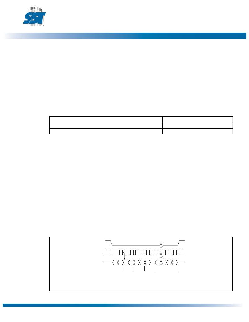
�Read-Status� Register� (RDSR)�
�The� Read-Status� register� (RDSR)� command� outputs� the� contents� of� the� Status� register.� The� Status� register�
�may� be� read� at� any� time� even� during� a� Write� operation.� When� a� Write� is� in� progress,� check� the� BUSY� bit�
�before� sending� any� new� commands� to� assure� that� the� new� commands� are� properly� received� by� the� device.�
�To� execute� a� Read-Status-Register� operation� the� host� drives� CE#� low,� then� sends� the� Read-Status-�
�Register� command� cycle� (05H).� Each� cycle� is� two� nibbles� long,� most� significant� nibble� first.� Immedi-�
�ately� after� the� command� cycle,� the� device� outputs� data� on� the� falling� edge� of� the� SCK� signal.� The� data�
�output� stream� continues� until� terminated� by� a� low-to-high� transition� on� CE#.� See� Figure� 19� for� the�
�RDSR� instruction� sequence.�
�CE#�
�MODE� 3�
�0�
�2�
�4�
�6�
�8�
�N�
�SCK� MODE� 0�
�SIO(3:0)�
�C1� C0� H0� L0� H0� L0� H0� L0�
�MSN� LSN�
�Status� Byte� Status� Byte� Status� Byte�
�H1� L1�
�Status� Byte�
�1359� F11.0�
�Note:� MSN� =� Most� Significant� Nibble;� LSN� =� Least� Significant� Nibble�
�C[1:0]� =� 05H�
�Figure� 19:� Read-Status-Register� (RDSR)� Sequence�
�?2011� Silicon� Storage� Technology,� Inc.�
�23�
�DS-25017A�
�04/11�
�发布紧急采购,3分钟左右您将得到回复。
相关PDF资料
SST38VF6402-90-5I-B3KE-T
IC FLASH MPF 64MBIT 90NS 48TFBGA
SST39LF802C-55-4C-MAQE-T
IC FLASH MPF 8MBIT 48-WFBGA
SST39SF040-70-4C-WHE
IC FLASH MPF 4MBIT 70NS 32TSOP
SST39VF1602C-70-4I-B3KE
IC FLASH MPF 16MBIT 70NS 48TFBGA
SST39VF200A-70-4I-MAQE
IC FLASH MPF 2MBIT 70NS 48-WFBGA
SST39VF3201-70-4I-B3KE-T
IC FLASH MPF 32MBIT 70NS 48TFBGA
SST39VF3201B-70-4C-B3KE
IC FLASH MPF 32MBIT 70NS 48TFBGA
SST39VF3201B-70-4I-EKE
IC FLASH MPF 32MBIT 70NS 48TSOP
相关代理商/技术参数
SST26VF064B
制造商:MICROCHIP 制造商全称:Microchip Technology 功能描述:3.0V Serial Quad I/O (SQI) Flash Memory
SST26VF064B-104-5I-MF
制造商:MICROCHIP 制造商全称:Microchip Technology 功能描述:3.0V Serial Quad I/O (SQI) Flash Memory
SST26VF064B-104-5I-SM
制造商:MICROCHIP 制造商全称:Microchip Technology 功能描述:3.0V Serial Quad I/O (SQI) Flash Memory
SST26VF064B-104-5I-SO
制造商:MICROCHIP 制造商全称:Microchip Technology 功能描述:3.0V Serial Quad I/O (SQI) Flash Memory
SST26VF064B-104-5I-TD
制造商:MICROCHIP 制造商全称:Microchip Technology 功能描述:3.0V Serial Quad I/O (SQI) Flash Memory
SST26VF064B-104I/MF
制造商:Microchip Technology Inc 功能描述:3.0V SERIAL QUAD I/O (SQI) FLASH MEMORY - Rail/Tube
SST26VF064BA
制造商:MICROCHIP 制造商全称:Microchip Technology 功能描述:3.0V Serial Quad I/O (SQI) Flash Memory
SST26VF064BA-104-5I-MF
制造商:MICROCHIP 制造商全称:Microchip Technology 功能描述:3.0V Serial Quad I/O (SQI) Flash Memory